Circuit Board Repair Pads
Pad via bga repair surface mount pads board integral circuit replace damaged method used Repair board circuit printed solder tools equipment pcb soldering process basic guide requirements any electronics Land repair kit, pcb pad repair kit
PCB pad repair kit dry film version for the repair of lifted pads on
Pcb pads askelectronics Pcb pad repair kit dry film version for the repair of lifted pads on Printed circuit board repair
4.7.4 surface mount, bga pad with integral via repair
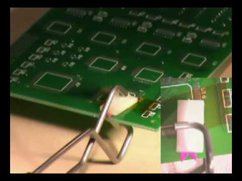
Routing mentor serpentine mostecDamaged pads instructables Repairing damaged or lifted pads on a circuit boardPcb pad repair epoxy version.
Pcb epoxy liftedHow to repair damaged printed circuit board pads : 9 steps (with Kit circuit repair professional board pad frames 2100 bga adhesive filmConcepts and terminology used in printed circuit boards (pcb.

What is a pad in pcb design and development
Hardware design with pads professionalRepair pad kit land pcb surface mount intertronics replacement What is a pad in pcb design and developmentHow to repair damaged printed circuit board pads?.
What is a pad in pcb design and developmentPcb pad repair epoxy Lifted circuit damaged repairingWhat’s the purpose of the larger metal pads on the sides of this blank.

201-2100 professional repair kit
Pads pcb circuit printed board smd concepts tracks boards engineering electrosoft soldermask silkscreen thru hole fig components terminology used .
.


